JustForex
Loading recent posts...

Sep 13, 2012

Intel Haswell Comes with 128 MB On-Package Cache


Intel’s decision to keep DDR3 memory for Haswell is in the users’ best interests as the price of such memory is continuously falling. The problem for the company was ensuring a large enough bandwidth for the powerful iGPU.

During this year’s IDF event in San Francisco, California, the company presented various aspects of the new architecture and an interesting bit of info is the fact that the chip will also benefit from a large on-package cache, AnandTech reports.

This cache is Intel’s solution for keeping the Haswell GT3 iGPU well fed. The buffer will be 128 MB in size and on-package means that the memory will not be on-die like the usual cache is, but there’s no clear info on the way it is actually designed.

Intel Haswell chip
Image credits to Intel

GeForce GK106-Based GTX 660 Standard and AMP! Edition


Traditional Nvidia add in board (AIB) video card manufacturing partner, well-known company Zotac is officially launching today its own implementations of the new GK106 GPU that features 960 CUDA cores and it’s being manufactured in TSMC’s 28nm technology.

The company’s “basic” GK106 card is the Zotac GeForce GTX 660 and this card has a slightly GPU overclock as the base frequency is rated at 993 MHz while the Boost option can up it to a high 1059 MHz. The second card launched today is the Zotac GeForce GTX 660 AMP! Edition that has its GPU clocked at high 1046 MHz base frequency right from the box.

Zotac’s AMP! Edition features a custom cooling system that will certainly help when the card’s Boost option is activated and the GPU clock is risen at 1111 MHz. The 2 GB of GDDR5 memory on both cards is unfortunately running at the default 6008 MHz effective frequency.


Zotac GeForce GTX 660 Video Cards
Images credits to Zotac

Zotac GeForce GTX 660 AMP! Edition Video Cards Specifications
Image credits to Zotac

Zotac GeForce GTX 660 Standard Video Cards Specifications
Image credits to Zotac


Gigabyte AB24BT 24" Ivy Bridge AIO Barebone System


Gigabyte has come up with a very interesting concept. We’re talking about a barebone that becomes an AIO system once the user chooses how much RAM memory he needs and chooses an LGA1155 CPU along with an HDD or an SSD.

The system supports Ivy Bridge and Sandy Bridge processors with a maximum TDP of 95 watts while the 2.5” HDD bay is actually a dock where the user can switch the drive with much ease. The official name of the product is Gigabyte AB24BT and it is built around Intel’s H61 chipset while featuring a nice 24” FullHD LED-backlit display with 2-point multi-touch support.

Gigabyte’s barebone also includes two 5W speakers along with a DVD-RW drive unit and a 4 in 1 card reader.


Gigabyte AB24BT AIO Barebone System
Images credits to Gigabyte

Zenithink N6 Arrive Soon as a 6-inch Android Smartphone


If you thought that Samsung’s Galaxy Note 2 was a large smartphone you should reconsider that.

A new, 6-inch Android-based smartphone is reportedly headed to shelves in the not too distant future, namely Zenithink N6. GizmoChina has got the chance to have a close look at the device, and suggests that it is rather bulky, especially when you look at it as a smartphone that should offer one-handed operations and should also fit in your pocket.

Unfortunately, no specific info on the phone’s hardware specifications has emerged so far, but more could become available next month or so. The device is only a bit smaller than the Google Nexus 7 tablet, yet it is certainly far larger than Apple’s new iPhone 5 model, which sports only a 4-inch touchscreen display. Stay tuned for more info on this handset.


Zenithink N6
Images credits to GizmoChina

Intel Successfully Ports Android 4.1 Jelly Bean to Its Medfield Chips


Android 4.1 Jelly Bean, the latest version of Google’s mobile operating system, is now working on Intel’s low-power Atom chips code-named Medfield, PCWorld reports.

Smartphones that are powered by Intel processors are already available for purchase around the world, yet they run under the Android 2.3 or Android 4.0 versions of the platform. There’s no telling on whether these devices will receive an update to Android 4.1, but it’s great news for Intel that they managed to successfully port the platform, as they are trying to gain more market share on the already crowded mobile space.

Orange, ZTE, Lava International, Lenovo and Megafon are some of the vendors who have already launched Intel-based smartphones, and more of them are expected to make similar moves soon, including Motorola, which has been acquired by Google last year.

Intel Medfield-based ZTE Grand X IN
Image credits to ZTE

Intel Core i7-4900 CPU Series Coming in Q3 2013


We reported here that there are strong chances Intel will not launch the top performing desktop version of the new Haswell architecture next spring and it seems like we were actually right about this.

AMD’s lack of a worthy x86 performance competitor seems to be the reason behind Intel’s delay. Intel is the type of company that likes to charge its customers “and arm and a leg” for every tiny performance improvement that its products are offering. The only way this sometimes changes is by the means of a surprising competing architecture that forces the company to innovate and offer innovations not only for money, but also to win back customers or not to lose them in the first place.

Intel is reportedly planning to launch its new top performing Haswell desktop processors in autumn of next year and this will also mark the introduction of the Core i7-4900 series. What’s interesting is that the Core i7-4900 series are actually Ivy Bridge-E processors, not Haswell. Ivy Bridge-E comes in LGA2011 form and will have support for DDR3-1866 memory along with a clock that’s probably going to end up higher than 4 GHz when Boost mode is active.

Intel Ivy Brigde E HEDT Processor slide
Image credits to BSN

World’s Most Efficient Intel Xeon Server Ever Built is AMD SeaMicro SM15000


AMD’s SeaMicro server division is well known for their Freedom Fabric connectivity technology where the I/O, storage and processing units are all being coordinated through a silicon PHY implementation developed by the latter.

SeaMicro used to build Intel-based servers, but once AMD acquired it, Opteron processors were also added to the list. Recently, AMD announced the SeaMicro SM15000 server and we’ve reported that here, but what we didn’t have were all the details and slides detailing the event. Hardware experts at Bridghtsideofnews.com have managed to get their hands on some interesting technological presentation slides that advertise what AMD calls “most efficient Inter Xeon server ever built.”, BSN reports. We wonder if HP’s own National Renewable Energy Laboratory (NREL) project is not the most efficient HPC data center anymore. Even so, AMD is able to deliver impressive density as its own servers take 74% less space than Intel’s own Sandy Bridge / Ivy Bridge Xeon server implementations. In fact, AMD’s SM15000 5 Petabyte storage cluster implementation uses 160 less operating system licenses than a classical Intel counterpart and 186 less power cables.

This is an amazing achievement from SeaMicro and AMD, but the most important aspects are the fact that the SM15000 uses only half the energy Intel’s implementation needs and costs exactly 50% less. Despite the fact that AMD’s Opteron may not offer superior performance to Intel’s Xeon Ivy Bridge processors, the Piledriver enhanced Opterons bring twice the CPU core and RAM density. Therefore, an Opteron powers SM15000 will have 2024 core per rack while the Intel version “only” brings 1024 cores. It will also offer 16,384 GB or RAM per rack while the Xeon Ivy Bridge implementation will “only” have a maximum of 8192 GB of RAM.

AMD logo
Image credits to AMD

AMD SeaMicro SM15000 Presentation
Image credits to BrightSideofNews

AMD SeaMicro SM15000 Presentation
Image credits to BrightSideofNews

Intel Haswell-EP Will Follow Ivy Bridge-EP with 14 Cores and 4-Channel DDR4


There is now information on not only the next-generation high-end EP platform, but also on the processor range that will debut after it. All thanks to the Intel Developer Forum.

These three days have been filled with announcements from Intel and the participants at its IDF San Francisco 2012 event, as well as attempts on AMD's part, and that of others, to distract people from that trade show. We doubt we'll find any sort of “counter-announcement” to the info that the folks at VR-Zone claim uncovered. The Intel Ivy Bridge-EP processor platform, scheduled for 2013, will succeed the Sandy Bridge-EP that, even now, hasn't been fully released. That was something we already knew, just like we knew that a 15-core Ivy Bridge EX CPU (Xeon E7 4800 V2) will debut around the middle of 2013, compatible with socket 2011. What we didn't know was that the “Haswell-EX” Xeon E7 4800 / 800 v3 will arrive in 2014 and will offer 16 to 20 cores. Afterwards, “Broadwell EX” Xeon E7 4800 / 8800 v4 will arrive, in 2015, with even more cores.

In the meanwhile, the existing 8-core Sandy Bridge EP Xeon E5 2600 / 4600 will pass the torch to a 10-core 3.2+ GHz Ivy Bridge EP Xeon E5 2600 / 4600 v2 (2014). Again, a different pin-out will be used, but the same dimensions as socket 2011. After that, the 2015-bound Haswell EP Xeon E5 2600 / 4600 v3 will possess 14 cores, 4-channel DDR4-2133 memory support, quad-QPI links (9.6 GT/s), the works. What we find curious is the progressive rise in core count. Although we admit that software can only get better at multi-thread performance, we can't help but feel that the rate of adding cores to CPUs, even high-end ones, is a bit fast.

There is also the matter of convenience: if Haswell-EP, with its power efficiency benefits (foreshadowed by 7-10W Haswell CPUs), can operate at TDPs of 145W (server) and 160W (workstation), adding the extra cores makes more sense than not using the space. It helps that the L3 cache (2.5 MB per core) can stay the same even under these conditions.

Intel logo
Image credits to Intel

Intel 16nm Manufacturing Process to Became 14nm – Advanced 10nm Coming in 2015


Intel is apparently now solely focused on mobile technologies while high performance desktop processors with ever rising high frequencies are not the company’s top priority anymore. The semiconductor giant takes the ARM threat very seriously.

We’ve reported here about AMD’s experiments with denser microchip designs and we’ve explained that you can make a design have a much smaller die and take up considerably less space on the wafer, but the frequency will not grow by much. We’re used to see that once a semiconductor company moves its designs on a more advanced and smaller manufacturing process, the frequency usually increases while the power consumption goes the other way around. The thing is that this is not an axiom, but rather a design choice. Of course, the transistors are smaller and consume less energy, but the company specifically places them further apart on the design so that there will not be any hot spots on the chip die. This makes the die bigger, but also allows the company to safely increase the working frequencies of the chips.

There are automated design tools that will place all the transistors and units as tight as possible while ensuring the chip works flawlessly. Such a design has a considerably smaller die that’s cheaper to manufacture, but will have significantly lower working frequencies. AMD is experimenting with these concepts as we detailed here, but Intel has also decided to go for increased density in the detriment of the high frequencies that would otherwise be attainable, Fudzilla reports.

Therefore, Intel decided to go for 14nm instead of 16nm manufacturing and the process bears the name P1272. This is the same name tag that was initially assigned to the 16nm process. The company says that its 14nm manufacturing process is still not ready for mass production, but it hopes it will be at the end of 2013 for a 2014 Broadwell launch. This is rather strange as we know Intel already has functional 14nm Broadwell processors. Moreover, during this year’s IDF event, Intel talked about its 10nm process, but all it said was the fact that it will be in mass production by 2015. We have our doubts that Intel will go so quick from 14nm to 10nm in two consecutive years.

Intel IDF 2012 Advanced Manufacturing Technologies Presentation
Image credits to Fudzilla

Nikon D600 DSLR 24.3-Megapixel Camera


We have known that it was coming since April (2012), and an August leak provided the ETA, but we didn't actually expect Nikon's D600 DSLR to match even overpowered products like Sony's Cyber-shot RX1 and Alpha A99.

Like those two, the Nikon D600 is designed with a 24.3 megapixel sensor, which means that images have 24.3 million pixels. In fact, every other asset of the camera is on par with those of the aforementioned competing products, as made clear by the product page. The ISO sensitivity is, naturally, among the most important things we have to mention: 100-6,400 is the “normal” range, but it can be extended to 50 – 25,600 when needed. The Multi-CAM4800 AF (autofocus) system, borrowed from Nikon’s D4, is another advantage, as it can be set to 9-, 21- and 39-point coverage. Speaking of which, the 100% coverage viewfinder displays whichever AF mode happens to be selected, so that owners needn't remove the camera from their eye when trying to catch a good shot. Thus, 3D subject tracking is easier than ever, and this goes for both large and small subjects. That said, the scene and face recognition system deserves a mention as well. Thanks to its ability to analyze 2,016 pixels for brightness, colors and other info, it can help with autofocus and auto exposure.

As for actual hardware details, the 760g camera (without battery) is equipped with two SD cards (SDXC and UHS-I), USB, HDMI, a 3.2-inch 921k-dot LCD (automatic brightness control) and, optionally, a WU-1b Mobile Adapter. Nikon D600 should capture images in singular or multiple-shot mode, as well as Full HD 1080p video in 24p, 25p, and 30p, plus 60p, 50p, and 25p in 720p. Sales will start this month (September 2012) and the price is the greatest advantage over Sony's near-$3000/3000 Euro demands. The body of D600 goes for $2,099.95 / 1624 – 2,000 Euro / £1,955.99. The AF-S NIKKOR 24-85mm f/3.5-4.5G ED VR lens will add $600 / 464 – 600 Euro / £400, while the WU-1b will ship for $59.95 / 46 – 59.95 Euro / £64.99.
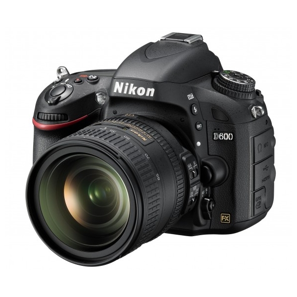
Nikon D600 camera
Image credits to Nikon

Twitter Delicious Facebook Digg Stumbleupon Favorites More

 
Design by Free WordPress Themes | Bloggerized by Lasantha - Premium Blogger Themes | coupon codes
`