JustForex
Loading recent posts...

Jun 28, 2012

Modbook Pro, Probably the Best Tablet in the World


Los Angeles-based company, Modbook Inc., has finally announced the specifications of its highly-anticipated Modbook Pro tablet-PC. The device will come to the market this year, and it will probably be one of the most powerful tablets in the world.

Years ago, Andreas E. Haas founded Modbook Inc. with the dream of building a high-quality tablet device that would have the power of a capable PC, the built quality and reliability of an Apple MacBook and that would be able to run Apple’s operating system. Back in 2008, Modbook Inc. went public and just ten days later Lehman Brothers went bankrupt, thus proving that the American government allowed financial companies to run rampant with no regard to the U.S. citizens’ well-being. The financial crisis hit the company very hard, and after years of work and restructuring, Modbook Inc. is now able to present the first information on the long-awaited Modbook Pro tablet computing device. Our users should know that the Modbook concept was presented years before Apple launched the first iPad, and that it was the first vision of an iOS-powered tablet-PC-like device. Today’s Modbook Pro tablet will encapsulate the original hardware inside the latest model of Apple’s MacBook Pro 13.3”, but all will be in the tablet form.

Modbook’s impressive tablet will ship with a Wacom digitizer pen that delivers 512 levels of pen pressure sensitivity that the company claims is more than any other tablet computer on the market can offer. The ForceGlass screen will provide an etched, paper-emulating drawing surface on the 13.3” screen, featuring a 1280 by 800 pixel resolution. We’re already used with FullHD screens on 10” tablets, but we’re going to let this one slide, as Modbook’s uniqueness resides in many different innovations and not an increased screen resolution. The initial hardware configuration will include an Intel Core i5 processor running at 2500 MHz with up to 16GB or RAM memory, and a 2.5” 1TB HDD or a 960 GB SSD. There is also a SuperDrive DVD burner along with one Gigabit Ethernet port, one FireWire 800 port, one USB 3.0 port, one Thunderbolt connector, an SDXC card slot, and one combo audio connector, just like the original Apple MacBook Pro.

The secret of the Modbook Pro tablet is the fact that the company practically takes an original Apple MacBook Pro apart and sticks it into a custom-made tablet enclosure. Apple’s original warranty is thus now void, but Modbook Inc. will issue a new warranty for the Modbook Pro tablet. Using Apple’s BootCamp, Modbook Pro tablet owners will be able to install Microsoft’s Windows 7 operating system. The Modbook Pro tablet is a device targeting drawing and CAD professionals, or simply tablet and Apple enthusiasts that are willing to pay a considerable premium price over the already high price of the MacBook Pro. Pricing is yet to be announced, but we’re curious how well ModBook’s interesting idea will sell.

ModBook Pro tablet
Image credits to ModBook Pro

ModBook Pro tablet
Image credits to ModBook Pro

ModBook Pro tablet
Image credits to ModBook Pro

ModBook Pro tablet
Image credits to ModBook Pro

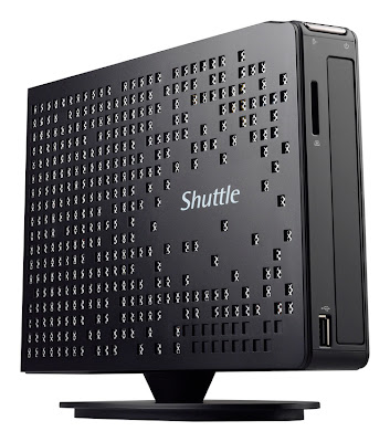
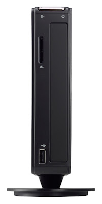
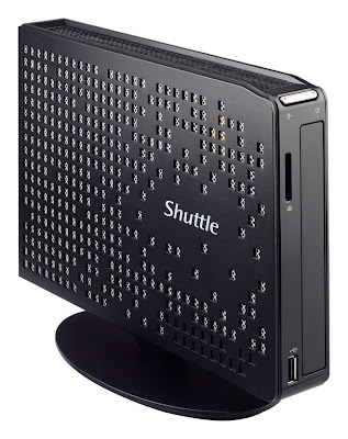
Shuttle Intros AMD Radeon-Powered Fanless Slim PCs


Shuttle, Well-known mini-PC manufacturer Shuttle has just announced the new Slim PC model XS35 as reported by Fanlesstech. This one comes with an Intel Atom D2700 dual-core processor, but it has AMD’s Radeon HD 7410M graphics card to help deliver acceptable 3D graphics.

Intel’s Atom D2700 is a dual-core Cedar Trail processor with HyperThreading enabled, that can handle four threads with modest performance. It comes with a single-channel DDR3 memory controller that can work with DDR3-800 MHz memory. Shuttle’s Slim PC XS35 is a completely fanless device that is certified for full 24-hour use and comes complete with an optional ODD bay for a slim DVD or Blu-Ray drive. Maximum power consumption is rated at 27 watts, and there are two SO-DIMM slots along with one 2.5” HDD bay.

Pricing is slated at €172 excluding the value added tax. This is about $214 for the American buyers. The XS35GTA V3 model coming with AMD’s Radeon HD video card is priced a little higher, at €233 ($290).

Shuttle SlimPC XS35V3 and XS35GTA V3 (powered by Atom D2700 and AMD Radeon HD 7410)
Image credits to Shuttle

Shuttle SlimPC XS35V3 and XS35GTA V3 (powered by Atom D2700 and AMD Radeon HD 7410)
Image credits to Shuttle

Shuttle SlimPC XS35V3 and XS35GTA V3 (powered by Atom D2700 and AMD Radeon HD 7410)
Image credits to Shuttle

Shuttle SlimPC XS35V3 and XS35GTA V3 (powered by Atom D2700 and AMD Radeon HD 7410)
Image credits to Shuttle

Shuttle SlimPC XS35V3 and XS35GTA V3 (powered by Atom D2700 and AMD Radeon HD 7410)
Image credits to Shuttle

Shuttle SlimPC XS35V3 and XS35GTA V3 (powered by Atom D2700 and AMD Radeon HD 7410)
Image credits to Shuttle

Google Nexus 7 Is Official, Pre-Order Now, Ships in Two Weeks


During its annual developer-focused conference, Internet giant company Google has launched its first Android tablet. The new device has a 7” diagonal size and sports a 1280 by 800 pixel resolution.

This is the first 7” tablet that’s being endorsed and marketed by one of the world’s biggest IT companies. Steve Jobs’ Apple has always mocked the 7” diagonal size and said many times that 7” tablets are not really tablets and, although in a much more humble manner, we tend to agree with him. Microsoft’s recently presented Surface tablet keeps up with Apple and features a diagonal of more than 7”, and it also brings other innovative features, such as a foldable keyboard/tablet cover. Therefore, Google is left alone by the big league tablet players on the 7” tablet front and it only competes with the likes of Acer, Samsung and ASUS.

The manufacturer behind Google’s Nexus is, in fact, the Taiwanese mainboard manufacturer called ASUS, the maker of the famous Transformer tablets. Just like Acer’s Iconia A110, the new Google Nexus is powered by a quad-core Tegra 3 or Tegra 4 + 1 SoC and features 1 GB of system RAM memory. The screen is a little better than Iconia A110's, as Acer’s tablet only has a 1024 by 600 pixel resolution. The Nexus 7 has an IPS led backlit screen that’s somewhat protected by Corning’s special glass. It also features a rather mediocre 1.2 MP front-facing camera, Wireless N, Bluetooth, Micro USB and a NFC chip. Compared with Acer’s Iconia A110, the Google Nexus 7 is 30 grams lighter, weighing just 340 grams. That’s about 0.75 pounds for the new Google tablet, although we’d rather carry 30 grams more and have the 2 MP webcam sported on the Iconia A110.

Nexus 7 features a rather large and capable 4325 mAh battery that is rated for 8 hours of active use. This is considerably larger than Iconia’s 3420 mAh battery. There is also a GPS inside, a Magnetometer, Gyroscope, Accelerometer and a Microphone, but no HDMI, unfortunately. It would have been nice to have some output options like Acer’s HDMI with DualDisplay support on the A110. The tablet is running Android 4.1, which is the "Jelly Bean" version that everybody is talking about. There are only 8 GB of flash storage inside, but, overall, Google’s Nexus 7 only brings good news, as the $199 price will force the price down on less popular devices like Acer’s Iconia that we’ve been talking about. There is also a $249 Nexus 7 version that comes with 16 GB of flash storage, but we find the lack of a microSD slot to be quite a disappointment. Priced at about €159 for the 8 GB version and €199 for the 16 GB model, Google’s Nexus 7 has just raised the bar in the cheap 7” tablet market niche.


The pre-order prices vary in different areas of the world, as Google identifies the location of your IP address.

The company will reportedly ship the desired toy in about 2 or 3 weeks from the pre-order date. In the United States, the prices are exactly as we said before, and that’s $199 USD for the 8-GB version and $249 USD for the 16-GB model. One thing that raised our eyebrows is the fact that Google is completely fair and doesn’t charge the British the same numerical value in pounds, but it only charges £159 for the 8-GB model and £199 for the 16-GB one.

Canadians will have to shell out $209 CAD for the cheapest version and $259 CAD for the better-endowed model. In Australia, Nexus 7 is priced at $249 AUS and $299 AUS, respectively.

ASUS Google 7" Nexus 7 Android 4.1 Tablet
Image credits to AnandTech

ASUS Google 7" Nexus 7 Android 4.1 Tablet
Image credits to AnandTech

ASUS Google 7" Nexus 7 Android 4.1 Tablet
Image credits to AnandTech

ASUS Google 7" Nexus 7 Android 4.1 Tablet
Image credits to gizmologia

ASUS Google 7" Nexus 7 Android 4.1 Tablet
Image credits to gizmologia


Jun 27, 2012

Android 4.1 Jelly Bean on Galaxy Nexus, XOOM and Nexus S in Mid-July


While announcing the new flavor of Android, namely 4.1 Jelly Bean, Google also confirmed its availability for Ice Cream Sandwich-based devices.

Starting with mid-July, the owners of Galaxy Nexus and Nexus S devices will get a taste of it, the same as those who own a Motorola XOOM tablet. The platform will be released along with the Android 4.1 source code, yet developers can already download and play with the updated SDK. The new OS flavor comes with a host of new features, including UI changes, Google now, updated camera app, improved notifications system, better performance, and more.

You can have a look at how the new platform can fare when compared to Ice Cream Sandwich on the Galaxy Nexus in the video above. The user experience will certainly be improved, but don't expect to observe the difference as obvious as in this slow-motion clip.


So in Jelly Bean, we put a lot of effort into making devices feel fast, fluid and smooth. This is what we call Project Butter.
Video credits to GoogleMobile

Android 4.1 Jelly Bean Now are Official


Today, Google has unveiled to the world the next flavor of its mobile operating system, Android.

Jelly Bean, the new of version, Android 4.1, comes with a new user interface, as well as with a set of new features meant to improve the overall user experience with the platform. Among these, we can count Project Butter, destined to improve the overall performance of the platform, as well as its response time. Better animations are also included in the new OS version, along with better CPU management, for increased response.

Users will be able to dynamically resize widgets on the homescreen, and can also remove them by simply flicking them off the screen. Apps can be removed the very same way. The camera app was updated as well, and new notifications are available, enabling users' email or call straight from them. Google’s Speech Recognizer was included into the mix too, along with a new search feature, Google now.

Android 4.1 Jelly Bean
Image credits to Engadget

Xeon Phi and AMD’s GCN Squeezing Nvidia’s TESLA


Intel’s Xeon Phi seemed like a doomed architecture back when Intel was attempting to compete with the likes of ATi and Nvidia. The company even scrapped the Larabee project, but all that work was not thrown away.

Intel redirected the use of their multiple core architecture towards high performance computing. We believe that much of the work was done on the software side, as Intel’s main purpose was to make software integration much easier for HPC users. The idea is a good one and the result is practical, although we’d rather have anything but x86 inside. For now, if Intel Xeon Phi x86 offers the better result, it deserves all the credit. Nvidia’s main problem is the fact that CUDA takes a whole lot of work to program for and that their new Kepler architecture is less powerful where raw computing power is involved. Therefore, a science center must pay for thousands of man-hours to port an application source code from x86 to CUDA just to take advantage of Nvidia’s Tesla. This is the added cost of choosing an Nvidia Tesla accelerator card for you server or supercomputer. Not only does the center have to pay for the extra man-hours of coding, but the final implementation and start usage of the server is also delayed by weeks or even months.

Intel brags that porting your code to its MIC accelerators will not take more than just a few days. Considering that the performance of the current Xeon Phi version is almost equal with Nvidia’s Kepler-based Tesla, the server owner will think twice before sticking Tesla cards inside, considering the additional funds he must provide for all the software optimization work. So what’s there left for Nvidia to do? If only Nvidia’s Kepler were faster. There is one faster card where DP FP64 is concerned, and that is AMD’s Tahiti GPU.


The second problem Nvidia has with its new Kepler architecture is that its raw compute power is actually less impressive than the company’s previous architecture.

Sure, Kepler is easier to program for and it is actually able to run a basic operating system, but the raw power would have made it stand tall ahead of Intel’s new MIC product line. Their main problem is that Intel touts 1 TFLOP of real-world double-precision (FP64) performance with its first iteration of Xeon Phi cards.  AMD stands quite alright in that perspective, as the current Radeon HD 7970 Tahiti GPU is able to deliver 947 GFLOPs for a much lower price than Xeon-Phi, while the new Radeon HD 7970 GHz Edition actually surpasses Intel’s goal by a significant margin of about 12%. Offering this much performance without any “professional” price tag is quite an achievement for AMD’s team. In fact, Nvidia’s top performing part when DP FP64 performance is concerned, is the Fermi-based Tesla M2090 card that is rated with a real-world double-precision (FP64) performance of 665 Gigaflops or 0.66 TFLOP.

How did Nvidia end up with a new generation of GPU compute accelerators that are slower than the previous generation? The answer is that Nvidia was not targeting DP FP64 performance with their current Tesla generation, and that they built the new Tesla K10 GPU compute cards using two Kepler GPUs. Thus, Nvidia’s K10 is able to achieve an impressive peak of 4.6 TFLOPs of single-precision compute performance. That’s 343% the performance of the Fermi-based Tesla M2090 card, but that’s not what Intel is offering. Remember that Intel emphasizes on double-precision FP64 performance rather than on single-precision.


Unfortunately, Nvidia’s DP PF64 performance with its Kepler GPU is over 6 times slower than what Fermi is able to put out. Kepler’s DP FP64 performance sits at just 95 Gigaflops, or 0.09 TFLOP.

The cards are clearly targeted at different applications, and at this point we believe that Nvidia would have been better off with a 28-nm-based Fermi with increased performance and lower thermals. Practically, a dual-GPU Fermi Tesla card built with 28-nm GPUs, but clocked at the same frequencies would be able to put out over 1.3 TFLOPs of DP FP64 performance. Nvidia could really pull this one out of their hat if the company decided to take this route. Now, many of our readers are probably thinking about the possibility that Nvidia could combine the best of both architectures and achieve the impressive single-point performance of Kepler and the high DP FP64 performance of Fermi. We believe that that’s exactly what Nvidia’s K20 is going for. The GK110 GPU inside will most likely provide competitive DP FP64 performance and even better single-point raw power.

Therefore, while Intel used its clout and money to kick Nvidia’s Tesla out of some of the supercomputers and servers that are now being built, Nvidia might strike back with a new set of Tesla products that will offer much better performance. It is also important to note that with Intel’s Xeon-Phi we’re talking about theoretical performance, as the cards are not out yet, while Nvidia’s Tesla K10 cards are up for grabs. Nobody can deny Intel’s performance achievements, and we believe that the simpler method of Xeon-Phi coding and optimization is a considerable advantage over Nvidia’s CUDA. On the other hand, Intel will have a tough road ahead if the next TESLA K20 card offers 1.7 or 1.9 TFLOPs of DP FP64 raw computing power.


Nvidia is not all defenseless before Intel’s money, market influence, software development, process manufacturing superiority and the general success of the Xeon Phi.

It’s obvious that Intel executed beautifully the remains of its Larabee project and the Knights Corner, MIC or Xeon Phi, whatever you’d like to call it, is, at the moment, an interesting product. We’re sure there’s a great deal of marketing and PR talk in Intel’s claim that porting applications to Xeon Phi is only a “matter of days,” instead of weeks or months. Nvidia has two main strong points now. The first one is the fact that their upcoming GK110 GPU that will power the Tesla K20 card is set to bring more than three times the DP FP64 performance of Nvidia’s previous Tesla generation powered by the Fermi architecture. We know that the Tesla M2090 Fermi-based GPU compute accelerator card is able to process a strong 0.66 TFLOPs of DP FP64 operations, and if the new K20 will be rated at over 1.9 TFLOPs, Intel’s Xeon Phi doesn’t look so powerful anymore.

Intel can brag and sing about their easy porting advantage of Xeon Phi all day, but no supercomputer maker is going to give up a 100 PFLOPs performance power and limit the project to 50 PFLOPs just because it’s easier to port. Supercomputing clients usually have very complex projects to run on their mega servers, and if one technology can deliver the result in one month, while the other will deliver it in twice the time, we have a hard time believing that the client will choose the slower hardware. The second strong point the Kepler-CUDA-GK110 combination gives Nvidia is exactly the continuity of the platform itself, and the fact that CUDA porting could be actually already done before GK110 reaches the client.


Nvidia’s way is the CUDA way and the true fact is that a lot of coding and optimization work is needed to fully enjoy the performance of Nvidia’s TESLA cards.  HPC clients might see Intel’s easier Xeon Phi coding as a way to reduce the cost of software coding that needs to be done.

On the other hand, HPC clients really care about performance. We have a hard time deciding if software coding money savings are more important than the end performance of the installation. We’re inclined to believe that, in the HPC or supercomputing world, money is usually not an issue and, more importantly, the small amount of money that software porting and optimization represents is not as important when compared with the total cost of the hardware and implementation. Considering that we’re talking about tens of thousands of dollars worth of man-hours doing coding and optimizing, the client paying for the server might give Intel’s Xeon Phi a thought if the performance were the same. The thing is that performance is not going to be the same. If Nvidia achieves its targets with the GK110 GPU, the DP F64 performance will be almost twice what Intel’s Xeon Phi brings to the table.

Some might wonder what’s the point in going for Kepler now. Why not wait for Xeon Phi or TESLA K20? The answer is that, if you want your supercomputer ready at the end of this year, you can safely go with Nvidia’s TESLA K10 that’s based on the new Kepler architecture. Sure, there is more CUDA programming to do, but you’ll be able to have you server ready much earlier than if you wait for Xeon Phi or TESLA K20. Having the final installation ready faster is only one of the advantages TESLA K10 offers. The second advantage is that, if you’ve ported your applications in CUDA and you’ve already had them optimized for the Kepler architecture, you can simply swap the TESLA K10 card with the K20 models when they hit the market.

Once this upgrade is finalized, your supercomputer will likely have 30 times the DP FP64 raw computing power compared with the initial Kepler K10 installation and more than 3 times the raw power of a similar Xeon Phi installation. There is nothing Intel can do this year or the next that would allow it to achieve a doubling of Xeon Phi’s DP FP64 performance and, from a pure performance point of view, Nvidia’s GK110 is a definite winner. Once we factor in AMD’s GCN, we’ll clearly see why Nvidia’s TESLA is being squeezed hard in the HPC market, but this will follow in the sixth part of our GPU compute analysis.

Intel Phi Logo
Image credits to Intel

Intel Xeon Phi Coprocessor Accelerator Card
Image credits to Intel

Nvidia TESLA K10 Card
Image credits to NVIDIA

Nvidia TESLA K20 Card based on the GK110 GPU
Image credits to NVIDIA

Nvidia TESLA K10 & K20 Performance Targets
Image credits to Hardware.fr


Jun 26, 2012

Adobe Brackets, an Open Source Code Editor Built in HTML, CSS, JavaScript


Adobe is very keen on HTML5 and the open web in general. This isn't just PR talk, it realized that Flash won't cut it for a lot longer and started supporting HTML5 in a big way. One example is the Brackets code editor which is available under an MIT license on Git Hub.

The editor is intended for HTML, CSS and JavaScript, but it's in the early stages and a lot more functionality is planned. What's more, modularity and extensibility are at the core of the design and there's no reason why users can't expand the editor's functionality to support more languages. Of course, HTML editors are a dime a dozen, what makes Brackets special is that it's actually built with HTML and JavaScript. In fact, the Adobe developers use Brackets to code for the editor in the most extreme example of eating your own dogfood.

For now, Brackets is available as a stand-alone app, i.e. it doesn't run in the browser, since some of the APIs that handle local files aren't as robust as they need to be. But that is one big goal for the team. One interesting idea in Brackets is that everything should happen in place. There are no complicated menus, no buttons, nothing. When you need to edit a few lines of CSS that are imported from another file, you can do it in-line while you're editing the HTML file. It gets better, everything you write you can test right away in a browser. Obviously, with web content that's always true. But what's great is that any change you do to the code is reflected, in real-time, in the browser, no refresh necessary. This should really speed up testing new layouts, colors, debugging features and so on. Brackets is a promising project, Adobe seems to be excited about it and the best part about it is that you can grab the source code and start using it and even improving it straight-away.

Adobe Brackets
Image credits to Adobe


Introducing Brackets a new open source code editor for the web. -- http://github.com/adobe/brackets
Video credits to Adobe

Sapphire Intros AMD Radeon HD 7870 FleX Video Card


Traditional AMD video card and mainboard manufacturing partner Sapphire has just announced the new Sapphire HD 7870 Flex Edition video card, on its official website. The new addition to Sapphire’s AMD Radeon product lineup comes with dual BIOS and the efficient Dual-X cooling system.

The new card features the cool AMD “Pitcairn” GPU that runs at the default 1000 MHZ frequency and uses 2 GB of on board GDDR5 memory clocked at 4800 MHz effective. For the enthusiasts gunning for maximum performance, a new version of the Sapphire’s TriXX overclocking tool is also added in the box along with the standard accessories.

There are four heatpipes taking care of the GPU cooling and two fans that blow air through the cooling fins. The card occupies two adjacent expansion slots and features HDMI 1.4a, dual DVI and DisplayPort connectivity on the I/O panel.


Sapphire AMD Radeon HD 7870 FleX GHz Edition
Images credits to Sapphire

Coming in Q3: AMD 4GHz Vishera FX 8350


AMD’s Piledriver architecture is bringing a whole lot of improvements to the original Bulldozer core. In fact, Piledriver is exactly what Bulldozer was supposed to be when it was first launched a year ago.

Reported by FudzillaAMD is planning a Q3 launch for its Piledriver-based FX 8350 processor. We believe that if Piledriver’s enhanced clock mesh seen in Trinity is applied to the FX processors also, the highest clocked model will most likely surpass, or at least equal, the 4 GHz frequency. The SOI manufacturing enhancements, along with the architecture improvements brought by Piledriver, have managed to get AMD’s APUs from 2,9 GHz to a high 3,8 GHz. Llano’s top model was clocked at a base frequency of 2900 MHz, while desktop Trinity processors are expected to work at frequencies of around 3800 MHz. That’s a 31 percent frequency improvement. We don’t expect AMD’s FX Piledriver processors to have a base clock of 4,7 GHz, but we do see the possibility of a 4 GHz base clock that would represent only a 11 percent increase over FX 8150’s base clock.

The desktop Trinity processors have a usual maximum TDP of 100 watts, but on the high end AM3+ camp, a TDP of about 140 watts is quite high, but not unheard of. Basically, if AMD manages to get the same clockspeed improvements on the AM3+ platform as they did on the FM2 architecture, the new Vishera 32nm processors will be able to reach at least the 4 GHz mark. Back in the days of Pentium 4 we were used to hear uninformed amateurs say that they bought Intel processors because they were cool, lasted long and worked at a higher frequency. Once AMD manages to “hypnotize” buyers with its marketing team, the new Volan platform should achieve high sales on the same principle. The CPUs will work at very high frequencies and that’s a fact. The irony dictates that they will be just as “cool” as Pentium 4 used to be and will last longer than Intel’s Ivy Bridge CPUs, just as Intel’s Pentium 4 CPUs lasted longer than AMD’s Athlon64.

AMD's FX 8150 Processor
Image credits to Legitreviews

Test: 3 Tb/s Wireless


There is a great deal of expectation when we talk about the new wireless devices belonging to the novel 802.11ac standard. It was said that WirelessAC is the first “Gigabit Wireless” standard, but it seems that scientists are not satisfied with the results and are working hard at the “Terabit Wireless” standard.

We don’t see 802.11ac as true “gigabit wireless,” because when using a single antenna on the AP and a single antenna on the receiving device, only 0.4 Gb/s data rates can be achieved. So we could say that we’re not satisfied with the current WirelessAC standard either. Scientists at NASA and many other universities in China, US and Israel have reported by Gizmodo tested a wireless signal able to transfer data at an amazing 2.56 Tb/s data rate.

The teams were able to pack eight data streams in the same single signal using orbital angular momentum (OAM). The results were first published in Nature magazine.

orbital angular momentum graph
Image credits to Engadget

Acer Sandy Bridge NetBook


Acer has decided to build a decent netbook, and that’s probably detrimental to the usual battery life expected from netbooks in general. The new device is powered by a modest-performing Celeron B877 processor and features a 11.6” screen.

The new netbook from Acer, Fudzilla reported quite a bit heavier than the usual netbook, but unfortunately it doesn’t feature the useful DVD-Writer. In fact, the TravelMate B113 is heavy enough not to fit in the UltraBook category either, but that is also excluded by the device’s thickness. The TravelMate B113 is a very peculiar device. It doesn’t look like an UltraBook, can’t last as long as a netbook, and it doesn’t have a propped ODD drive just like any notebook should have. This is device clearly targeted for the cash-strapped buyers that need more performance than a netbook can provide, but that don’t mind the lower battery life and the lack of the ODD.

The new TravelMate B113 series feature 4 GB of DDR3 RAM memory, a 500 GB hard disk drive, Wireless N and USB 3.0 connectivity, along with HDMI and a 4400mAh battery. The screen features the mediocre 1366 by 768 pixel resolution and the whole thing weighs in at 1.88 Kg. That’s about 4.14 pounds, and it is clearly too much to be considered an UltraBook. In our humble opinion, Acer could have included an optical disc drive in the design, as there are quite a lot of laptops that come with an ODD in the €450 ~ €560 price range of the TravelMate B113. In US dollars, that is around $563 to $700, which is quite pricey by our standards. The more capable versions come with a 1.3GHz Pentium B967 or a Core i3-2377M working at 1.5GHz.

Acer TravelMate B113
Image credits to Fudzilla

Acer TravelMate B113
Image credits to Fudzilla

RSA SecurID bypassed, Access Cryptographic Keys only in 13 Minutes


Experts from France, Italy, the UK, and Norway have released the results of a study which demonstrates that the flaws present in many of the popular security devices, such as the RSA’s SecureID 800, can be leveraged to obtain the precious cryptographic keys.

In a paper called “Efficient padding oracle attacks on cryptographic hardware,” researchers Romain Bardou, Lorenzo Simionato, Graham Steel, Joe-Kai Tsay, Riccardo Focardi and Yusuke Kawamoto detail the vulnerabilities that expose the imported keys from various cryptographic devices that rely on the PKCS#11 standard. They describe the method they used, the padding oracle attack, as a “particular type of side channel attack where the attacker is assumed to have access to an oracle which returns true just when a chosen ciphertext corresponds to a correctly padded plaintext under a given scheme.” By creating an optimized version of Bleichenbacher’s attack, the researchers have been able to prove that tokens such as the RSA SecurID, the Aladdin eTokenPro, the Gemalto Cyberflex, the Safenet Ikey 2032 and the Siemens CardOS can be cracked in a short period of time.

Surprisingly, the attack in the RSA’s device took only 13 minutes to complete, while the ones on Aladdin and Siemens took about 21 minutes. Safenet and Gemalto tokens were cracked in 88, respectively 92 minutes. The initial variant of the Bleichenbacher attack required millions of decryption attempts, explained Matthew Green, a research professor at Johns Hopkins University. However, the new version only requires thousands or tens of thousands of attempts. This paper is just one of many that show that the PKCS#1v1.5 padding for RSA encryption is highly insecure, a fact reinforced by Green, who believes that the past two years haven’t been the best for the industry.

The most worrying thing is that tokens that rely on this technology are utilized by numerous organizations to access restricted networks and perform other sensitive operations. That’s why the scientists recommend a few countermeasures to the Bleichenbacher and Vaudenay attacks.

Oracle details and attack times
Image credits to Project-Team Prosecco

Jun 25, 2012

AMD Fusion APUs 500% is Faster than Intel’s CPUs in Musemage


When it comes to photo processing, GPU accelerated compute power has a very high performance potential. Depending on the architecture in question and the API used, the result can be amazing.

AMD’s Llano seems to be a very capable APU, and despite the fact that it can already be called “last year technology” it demonstrates nice results. Software developers preference for open source APIs also puts AMD’s OpenCL capabilities in a better position than Nvidia’s CUDA. During this year’s AFDS, AMD posted some nice short videos exemplifying the performance improvement offered by the company’s GPU architecture. What the video doesn’t show is the impressive performance results that are achieved in real benchmarking.

William Van Winkle from Tom’s Hardware put AMD’s A8-3850 APU to the test and the result was that the Llano APU is over 5 times faster than Intel’s Core i5 Sandy Bridge processor using HD 2500 iGPU. The more impressive part is the fact that AMD’s Radeon HD 7970 GPU is over 25 times faster than the same Core i5 CPU.


Accelerated by the AMD Radeon™ HD GPUs, Musemage enables ultra-fast speed and real-time visual feedback. Its powerful batch processing tool makes it incredibly easy to process multiple pictures at one time, including adjusting, resizing and applying filters!
Video credits: AMD

AMD G-T16R Shows 300% Performance of the GeodeLX, Consume Less Power


Fabless CPU and GPU designer, Texas-based company AMD has launched today the company’s new G-T16R embedded processor, on its official website. The new wonder consumes an average power of 2.3 watts and offers over three times the performance of Geode LX.

Many of our readers will remember AMD’s Geode line of embedded processors that the company acquired from National Semiconductor. Back in 2002, AMD needed to buy a whole CPU team from National Semiconductor to be able to offer processors that were proper to fit thin industrial clients and manifested a power consumption of less than 10 watts. Now, AMD is able to offer APUs that consume roughly less than quarter of that value and offer 300% the performance. We should not forget that AMD’s Geode LX was a significantly improved version of AMD’s Geode GX2 and also has AES Encryption. A 3-fold performance improvement along with a 7% decrease in average power consumption and a 58% in chip footprint is quite amazing.

AMD’s Embedded G-T16R APU support Windows Embedded Compact 7, Green Hills INTEGRITY and Express Logic ThreadX operating systems and have enhanced connectivity option such as VGA and LVDS support for legacy applications and DVI, HDMI along with DisplayPort. The maximum TDP of the platform is 4.5 watts, and this includes the APU and the associated chipset. Both chips occupy only 890 square millimeters, which is about a quarter of a square inch. AMD’s older Geode LX embedded processors are supposedly going to be available until 2015 while the team that designed them was relocated from Longmont, Colorado to the new development facility in Fort Collins, Colorado.

AMD's G-T16R Embedded Platform
Image credits: AMD

AMD's G-T16R Embedded Platform
Image credits: Advantech

AMD's G-T16R Embedded Platform Diagram
Image credits: AMD

This is it, HP’s First AMD “Trinity” Desktop System


HP has been a strong supporter of AMD during the last years.  Now, the company is among the first big OEM builders to launch “Trinity”-based desktop computer systems.

HP has chosen AMD GPUs as their main 3D processing solution in the company’s mobile systems for years now.  Even Nvidia was telling us at a Kepler presentation some months ago that they were very happy HP decided to finally use Nvidia GPUs again. They were proud to include HP on Nvidia’s design wins board, but the thing is that the first Ivy Bridge notebooks launched by HP were still using AMD GPUs. HP’s SleekBook is one of AMD’s best examples of how a “Trinty” UltraBook can be better than an Intel-based one. Of course, the UltraBook moniker is only reserved for Intel-based mobile systems, but we must accept that HP’s “SleekBook” brand is simply cooler. After all these pro-AMD moves, it is no wonder that HP is one of the first big computer builders to launch AMD “Trinity”-based desktop personal computer systems.

The system is called HP Pavilion P7-1269C and is already available for $820. That’s about €653 for the European buyers, and it’s just the starting price for a whole range of various configurations. There are many hardware combinations available, such as AMD APU-5800K A10, A10-5700, 5600K-A8, A8-5500, A6-A4-5300 and 5400K when the CPU is involved. The motherboard is an MSI MS-7778 (Jasmine) FM2 Socket micro-ATX based on AMD’s A75 chipset. It is actually manufactured by Pegatron for MSI, and it’s quite strange for HP to provide such detailed info on the insides of its new system. The system comes equipped with 8GB of DDR3-1600 RAM memory. Here are the complete system specifications on HP’s own official website.


HP Pavilion P7-1269C Desktop Computer System (AMD "Trinity" based)


All Images credits to HP


AMD Fusion Server Brings 252% of MATLAB Performance Using OpenCL


AFDS 2012 event is proving to be very interesting and is clearly has much more serious impact on the computing industry as last year.

Now we even have AMD APU based  professional servers from Penguin Computing fited with proper software that will take advantage of the iGPU inside AMD’s Fusion APUs and offer considerable better results. In this case the demonstration is done on a Penguin Computing Altus 2A00 server that you can read full story in Penguin Computings' Website.

The system is powered by AMD’s Llano APUs, but we can expect Trinity versions to appear soon. In this particular case, Penguin uses Accelereyes’ software called “Jacket” that allows MATLAB to run on but the x86 core and the iGPU at the same time. The iGPU is able to deliver 52% better performance, but as the speaker emphasizes, the server is actually running two threads at the same time offering a combined performance of 252% the performance of just the x86 cores.

The user will be able to run two different threads in MATLAB at the same time. One will use the x86 cores and the other will use the OpenCL capabilities of the iGPU with the help of Accelereyes’ “Jacket” software. The demo is impressive as practically the productivity of the system is increased almost three times while there is a single APU inside.


AMD's Sasa Marinkovic and AccelerEyes' John Melonakos demo Matlab on OpenCL and the AMD Trinity APU, from the Experience Zone at AFDS 2012. 


For more information, visit: http://bit.ly/AFDS-D and http://www.accelereyes.com/

Jun 22, 2012

Galaxy Nexus HSPA+, the First Phone with Android 4.1 Jelly Bean


Google is indeed gearing up for the release of a new version of its Android platform, and a leak coming from the company itself confirms it.

The Galaxy Nexus HSPA+, which is being sold through Google Play Store, has been listed on the website as “the first phone with Android 4.1 Jelly Bean,” screenshots coming from Droid-life confirm. This is the latest Google phone out there, and it was only natural for it to receive the latest OS upgrade first, as tradition calls. 
Moreover, the checkout page on the webs store listed the phone with a new homescreen, in line with what was spotted on the Google I/O conference app screenshots. The mentioning was already pulled off the site, but rumor has it that Google might make an official announcement on the new platform release as soon as next week.


Jun 21, 2012

Apple Explains the Thunderbolt to Gigabit Adapter


If you’re looking to find out which computers support the Apple Thunderbolt to Gigabit Ethernet Adapter, where you can connect it, the requirements for using it, etc., Apple released a handy FAQ that answers all these questions, and more.

If you’re curious to know which Macs support this adapter, you should be happy to learn that all Thunderbolt-equipped systems are a go, so long as you have OS X Lion v10.7.4 or later installed. Macs released prior to June, 2012 that also boast a Thunderbolt connector will require Thunderbolt Software Update 1.2.1 to use this adapter.

You can connect this adapter to external devices, as well as directly to the port on your Mac. And, if you’re "daisy chaining" multiple devices, Apple says that at least one computer on the Thunderbolt chain needs to act as a host. This and much more can be found here, in the Apple Thunderbolt to Gigabit Ethernet Adapter: Frequently Asked Questions.


Twitter Delicious Facebook Digg Stumbleupon Favorites More

 
Design by Free WordPress Themes | Bloggerized by Lasantha - Premium Blogger Themes | coupon codes
`