JustForex
Loading recent posts...
Showing posts sorted by relevance for query Kepler. Sort by date Show all posts

Jun 27, 2012

Xeon Phi and AMD’s GCN Squeezing Nvidia’s TESLA


Intel’s Xeon Phi seemed like a doomed architecture back when Intel was attempting to compete with the likes of ATi and Nvidia. The company even scrapped the Larabee project, but all that work was not thrown away.

Intel redirected the use of their multiple core architecture towards high performance computing. We believe that much of the work was done on the software side, as Intel’s main purpose was to make software integration much easier for HPC users. The idea is a good one and the result is practical, although we’d rather have anything but x86 inside. For now, if Intel Xeon Phi x86 offers the better result, it deserves all the credit. Nvidia’s main problem is the fact that CUDA takes a whole lot of work to program for and that their new Kepler architecture is less powerful where raw computing power is involved. Therefore, a science center must pay for thousands of man-hours to port an application source code from x86 to CUDA just to take advantage of Nvidia’s Tesla. This is the added cost of choosing an Nvidia Tesla accelerator card for you server or supercomputer. Not only does the center have to pay for the extra man-hours of coding, but the final implementation and start usage of the server is also delayed by weeks or even months.

Intel brags that porting your code to its MIC accelerators will not take more than just a few days. Considering that the performance of the current Xeon Phi version is almost equal with Nvidia’s Kepler-based Tesla, the server owner will think twice before sticking Tesla cards inside, considering the additional funds he must provide for all the software optimization work. So what’s there left for Nvidia to do? If only Nvidia’s Kepler were faster. There is one faster card where DP FP64 is concerned, and that is AMD’s Tahiti GPU.


The second problem Nvidia has with its new Kepler architecture is that its raw compute power is actually less impressive than the company’s previous architecture.

Sure, Kepler is easier to program for and it is actually able to run a basic operating system, but the raw power would have made it stand tall ahead of Intel’s new MIC product line. Their main problem is that Intel touts 1 TFLOP of real-world double-precision (FP64) performance with its first iteration of Xeon Phi cards.  AMD stands quite alright in that perspective, as the current Radeon HD 7970 Tahiti GPU is able to deliver 947 GFLOPs for a much lower price than Xeon-Phi, while the new Radeon HD 7970 GHz Edition actually surpasses Intel’s goal by a significant margin of about 12%. Offering this much performance without any “professional” price tag is quite an achievement for AMD’s team. In fact, Nvidia’s top performing part when DP FP64 performance is concerned, is the Fermi-based Tesla M2090 card that is rated with a real-world double-precision (FP64) performance of 665 Gigaflops or 0.66 TFLOP.

How did Nvidia end up with a new generation of GPU compute accelerators that are slower than the previous generation? The answer is that Nvidia was not targeting DP FP64 performance with their current Tesla generation, and that they built the new Tesla K10 GPU compute cards using two Kepler GPUs. Thus, Nvidia’s K10 is able to achieve an impressive peak of 4.6 TFLOPs of single-precision compute performance. That’s 343% the performance of the Fermi-based Tesla M2090 card, but that’s not what Intel is offering. Remember that Intel emphasizes on double-precision FP64 performance rather than on single-precision.


Unfortunately, Nvidia’s DP PF64 performance with its Kepler GPU is over 6 times slower than what Fermi is able to put out. Kepler’s DP FP64 performance sits at just 95 Gigaflops, or 0.09 TFLOP.

The cards are clearly targeted at different applications, and at this point we believe that Nvidia would have been better off with a 28-nm-based Fermi with increased performance and lower thermals. Practically, a dual-GPU Fermi Tesla card built with 28-nm GPUs, but clocked at the same frequencies would be able to put out over 1.3 TFLOPs of DP FP64 performance. Nvidia could really pull this one out of their hat if the company decided to take this route. Now, many of our readers are probably thinking about the possibility that Nvidia could combine the best of both architectures and achieve the impressive single-point performance of Kepler and the high DP FP64 performance of Fermi. We believe that that’s exactly what Nvidia’s K20 is going for. The GK110 GPU inside will most likely provide competitive DP FP64 performance and even better single-point raw power.

Therefore, while Intel used its clout and money to kick Nvidia’s Tesla out of some of the supercomputers and servers that are now being built, Nvidia might strike back with a new set of Tesla products that will offer much better performance. It is also important to note that with Intel’s Xeon-Phi we’re talking about theoretical performance, as the cards are not out yet, while Nvidia’s Tesla K10 cards are up for grabs. Nobody can deny Intel’s performance achievements, and we believe that the simpler method of Xeon-Phi coding and optimization is a considerable advantage over Nvidia’s CUDA. On the other hand, Intel will have a tough road ahead if the next TESLA K20 card offers 1.7 or 1.9 TFLOPs of DP FP64 raw computing power.


Nvidia is not all defenseless before Intel’s money, market influence, software development, process manufacturing superiority and the general success of the Xeon Phi.

It’s obvious that Intel executed beautifully the remains of its Larabee project and the Knights Corner, MIC or Xeon Phi, whatever you’d like to call it, is, at the moment, an interesting product. We’re sure there’s a great deal of marketing and PR talk in Intel’s claim that porting applications to Xeon Phi is only a “matter of days,” instead of weeks or months. Nvidia has two main strong points now. The first one is the fact that their upcoming GK110 GPU that will power the Tesla K20 card is set to bring more than three times the DP FP64 performance of Nvidia’s previous Tesla generation powered by the Fermi architecture. We know that the Tesla M2090 Fermi-based GPU compute accelerator card is able to process a strong 0.66 TFLOPs of DP FP64 operations, and if the new K20 will be rated at over 1.9 TFLOPs, Intel’s Xeon Phi doesn’t look so powerful anymore.

Intel can brag and sing about their easy porting advantage of Xeon Phi all day, but no supercomputer maker is going to give up a 100 PFLOPs performance power and limit the project to 50 PFLOPs just because it’s easier to port. Supercomputing clients usually have very complex projects to run on their mega servers, and if one technology can deliver the result in one month, while the other will deliver it in twice the time, we have a hard time believing that the client will choose the slower hardware. The second strong point the Kepler-CUDA-GK110 combination gives Nvidia is exactly the continuity of the platform itself, and the fact that CUDA porting could be actually already done before GK110 reaches the client.


Nvidia’s way is the CUDA way and the true fact is that a lot of coding and optimization work is needed to fully enjoy the performance of Nvidia’s TESLA cards.  HPC clients might see Intel’s easier Xeon Phi coding as a way to reduce the cost of software coding that needs to be done.

On the other hand, HPC clients really care about performance. We have a hard time deciding if software coding money savings are more important than the end performance of the installation. We’re inclined to believe that, in the HPC or supercomputing world, money is usually not an issue and, more importantly, the small amount of money that software porting and optimization represents is not as important when compared with the total cost of the hardware and implementation. Considering that we’re talking about tens of thousands of dollars worth of man-hours doing coding and optimizing, the client paying for the server might give Intel’s Xeon Phi a thought if the performance were the same. The thing is that performance is not going to be the same. If Nvidia achieves its targets with the GK110 GPU, the DP F64 performance will be almost twice what Intel’s Xeon Phi brings to the table.

Some might wonder what’s the point in going for Kepler now. Why not wait for Xeon Phi or TESLA K20? The answer is that, if you want your supercomputer ready at the end of this year, you can safely go with Nvidia’s TESLA K10 that’s based on the new Kepler architecture. Sure, there is more CUDA programming to do, but you’ll be able to have you server ready much earlier than if you wait for Xeon Phi or TESLA K20. Having the final installation ready faster is only one of the advantages TESLA K10 offers. The second advantage is that, if you’ve ported your applications in CUDA and you’ve already had them optimized for the Kepler architecture, you can simply swap the TESLA K10 card with the K20 models when they hit the market.

Once this upgrade is finalized, your supercomputer will likely have 30 times the DP FP64 raw computing power compared with the initial Kepler K10 installation and more than 3 times the raw power of a similar Xeon Phi installation. There is nothing Intel can do this year or the next that would allow it to achieve a doubling of Xeon Phi’s DP FP64 performance and, from a pure performance point of view, Nvidia’s GK110 is a definite winner. Once we factor in AMD’s GCN, we’ll clearly see why Nvidia’s TESLA is being squeezed hard in the HPC market, but this will follow in the sixth part of our GPU compute analysis.

Intel Phi Logo
Image credits to Intel

Intel Xeon Phi Coprocessor Accelerator Card
Image credits to Intel

Nvidia TESLA K10 Card
Image credits to NVIDIA

Nvidia TESLA K20 Card based on the GK110 GPU
Image credits to NVIDIA

Nvidia TESLA K10 & K20 Performance Targets
Image credits to Hardware.fr


Dec 13, 2011

Nvidia Kepler Is On Track, Samples Arrived In-House


Even though AMD will most certainly be the first graphics card maker to release a 28nm GPU, Nvidia hasn’t abandoned the fight and has recently disclosed that Kepler is on track and that they have already entered into the possession of the first 28nm chip samples.

“We are on track with our Kepler roadmap. We have 28nm silicon in house now,” said Igor Stanek, Senior Product PR Manager at Nvidia during an interview with the Fudzilla website.

“Our transition to 28nm is going better than 40nm, and yields are better than our original plan,” concluded the company’s rep without going into any details regarding Kepler’s roadmap.

However, over the course of the last few months, multiple Nvidia representatives have said that the first Kepler-based graphics cards aren’t expected to arrive until Q2 of 2012, so this is probably the timeline that Stanek is referring to.

Before Kepler arrives, the GPU maker is expected to release a series of die shrinks of Fermi built using TSMC's 28nm fabrication process. 

The first chips based on the Kepler architecture were taped out by Nvidia at the beginning of September. 

Kepler is the code name used by Nvidia to refer to its next-generation graphics processing unit architecture, which, just like AMD's Radeon HD 7000 GPUs, will be manufactured using TSMC's 28nm fabrication process.

The new graphics core is expected to be more flexible in terms of programmability than the current Fermi architecture.

In the second half of 2010, Nvidia promised that Kepler, and its successor Maxwell, will include virtual memory space (allowing both the CPU and the GPU to use a unified virtual memory) and pre-emption support, as well as a series of other technologies meant to improve the GPU's ability to process data without the help of the system's processor.

According to previous Nvidia estimates, these changes, combined with the new manufacturing process, should deliver 3 to 4 times the performance per Watt of the Fermi architecture in double-precision 64-bit floating point operations.

Oct 27, 2011

Nvidia Kepler GPUs to be Announced in December Says Report


Nvidia seems to be making great progress with its next-generation graphics cards based on the Kepler architecture as a recent report to make its appearance on the Web states that the chip maker is planning to announce these GPUs in December of this year.

The DigiTimes report doesn't explain what it understands when it says “announce,” but most probably this means that Nvidia will showcase such a GPU at an event or press conference.

Availability will most probably still remain scheduled for 2012, just as various Nvidia representatives, have said over the time.

Before Kepler arrives the GPU maker is expected to release a series of die shrinks of Fermi built using TSMC's 28nm fabrication process.

The first chips based on the Kepler architecture were taped out by Nvidia at the beginning of September.

Kepler is the code name used by Nvidia to refer to its next-generation graphics processing unit architecture, which, just like AMD's Southern Islands GPUs, will be manufactured using TSMC's 28nm fabrication process.

The new graphics core is expected to be more flexible in terms of programmability than the current Fermi architecture.

In the second half of 2010, Nvidia promised that Kepler, and its successor Maxwell, will include virtual memory space (allowing both the CPU and the GPU to use a unified virtual memory) and pre-emption support, as well as a series of other technologies meant to improve the GPU's ability to process data without the help of the system's processor.

According to previous Nvidia estimates, these changes, combined with the new manufacturing process, should deliver 3 to 4 times the performance per Watt of the Fermi architecture in double-precision 64-bit floating point operations.

In the consumer market, Kepler-based graphics cards will most likely carry the GeForce 600 designation.

Jan 12, 2012

CES 2012: Nvidia Wanted to Showcase Kepler at the Fair, But Decided Not to


With AMD’s release of the 28nm Radeon HD 7970 at the end of last year, everyone’s attention has now turned towards the green camp, but Nvidia’s Kepler still seems to have a long way to go before it arrives, Jen Hsun Huang, the company’s CEO, advising us to be patient about it.

Reportedly, at some point in time Nvidia wanted to present a Kepler GPU at this year’s CES fair during Huang’s keynote speech, but in the end it decided not to.

This was a business decision according to Fudzilla who says that Kepler is actually in production and that the chip is scheduled for a H1 2012 launch, probably at the end of this quarter.

Jen Hsun Huang told the same publication that we need to be patient when it comes to its next-gen GPU, which does indeed seem to imply that we have quite a long wait ahead of us.

Kepler is the code name used by Nvidia to refer to its next-generation graphics processing unit architecture, which, just like AMD's Radeon HD 7900 GPUs, is manufactured using TSMC's high-K metal gate (HKMG) 28nm fabrication process.

The new graphics core is expected to be more flexible in terms of programmability than the current Fermi architecture.

In the second half of 2010, Nvidia promised that Kepler, and its successor Maxwell, will include virtual memory space (allowing both the CPU and the GPU to use a unified virtual memory) and pre-emption support, as well as a series of other technologies meant to improve the GPU's ability to process data without the help of the system's processor.

According to previous Nvidia estimates, these changes, combined with the new manufacturing process, should deliver 3 to 4 times the performance per Watt of the Fermi architecture in double-precision 64-bit floating point operations.


Sep 22, 2011

Nvidia Tapes Out Its First 28nm Kepler GPUs – Report

Nvidia is getting ready for the introduction of its first graphics cards based on the 28nm Kepler architecture and the company has recently taped out its first SKUs to be based on this design, according to a recent report to hit the Web.

The two cores are known under the code names of GK117 and GK107, and SemiAccurate reports these are both entry-level graphics chips.

The GK117 was the first of the two to arrive and, according to sources cited by the above-mentioned Website, is described as a hybrid between Fermi and Kepler which lacks an integrated display controller.

This is a rather odd occurrence as the code-name Nvidia used points out to a rather small core, so this can't be a Tesla GPGPU solution. The most likely explanation is that GK117 is a test chip for the 28nm Kepler architecture.

Moving to the GK107, the code name points to a GPU that should address the markets and price segments currently covered by GF108 and GF106.

If the information uncovered by SemiAccurate turns out to be indeed true, it seems like Nvidia may be in a bit of a pickle as it won't have any high-performance solutions based on the Kepler architecture ready in the first quarter of 2012.

In electronics design, the “tape out” term is used to describe the final result of the design cycle of a chip and means that the integrated circuit can be sent to the foundry for manufacturing the first physical samples.

These will then go through a number of spins as the design is further refined to eliminate any potential flaws that made their way into the integrated circuit.

This is usually a pretty lengthy process, so if Nvidia doesn't face any problems with the A0 silicon of the GK117 and GK107, these should become available sometime in April of 2012.

Kepler is the code name used by Nvidia to refer to its next-generation graphics processing unit architecture, which introduces a series of new technologies meant to improve the GPU's ability to process data without the help of the system's processor, while also delivering improved graphics performance.


Jun 7, 2012

Kepler GPUs on DELL Sooner Than We Think


DELL will most certainly equip its next 15.6-Inch XPS notebook with NVIDIA’s frontrunner, Kepler Quadro GPU, or so the supported graphic cards list found in 296.79 drivers says.

Kepler GPUs are using the 28nm technology to deliver speeds up to 1,006 MHz stock rating, or 1,058 MHz with GPU Boost. These are speeds for desktop workstations; the latest GTX 680M GPU for mobile devices can go up to 720 MHz. The 296.79 drivers package has been spotted online, available for download, and offers support for Windows 7, both x32 and x64 architecture.

What’s interesting about it is that the “NVDM.INF” file lists a bunch of supported GPUs from Kepler line (K series), amongst others. The driver version is 8.17.12.9679 and is dated 05/10/2012:

NVIDIA_DEV.0FFB.053E.1028 = "NVIDIA Quadro K2000M"
NVIDIA_DEV.0FFB.153E.1028 = "NVIDIA Quadro K2000M"
NVIDIA_DEV.0FFC.053E.1028 = "NVIDIA Quadro K1000M"
NVIDIA_DEV.0FFC.153E.1028 = "NVIDIA Quadro K1000M"
NVIDIA_DEV.11BC.053F.1028 = "NVIDIA Quadro K5000M"
NVIDIA_DEV.11BC.153F.1028 = "NVIDIA Quadro K5000M"
NVIDIA_DEV.11BD.053F.1028 = "NVIDIA Quadro K4000M"
NVIDIA_DEV.11BD.153F.1028 = "NVIDIA Quadro K4000M"
NVIDIA_DEV.11BE.053F.1028 = "NVIDIA Quadro K3000M"
NVIDIA_DEV.11BE.153F.1028 = "NVIDIA Quadro K3000M"

DELL Kepler Quadro Mobile NVIDIA Display Driver 296.79 for Windows 7
DELL Kepler Quadro Mobile NVIDIA Display Driver 296.79 for Windows 7 x64


Mar 12, 2012

Nvidia Kepler GK104 GPU Die Size Exposed – Report


The die size on Nvidia’s highly anticipated GK104 “Kepler” GPU was exposed recently by a Chinese website that apparently entered into the possession of an image depicting the company’s next-gen 28nm graphics core.

The picture, published just earlier today by Expreview, has the GK104 GPU standing next to a G92b graphics processor, which we already know it has a die size of 231 square millimeters.

Since the Kepler GPU pictured looks to be only slightly larger than the G92b, it seems that Nvidia’s new chip will be a great deal smaller than the company’s current Fermi GF110 and GF114 cores.

This also seems to be confirmed by some measurements revealed by Expreview, which state that the Kepler GPU packaging measures 40mm x 40mm, while its die is 17.2mm x 17.2mm, which makes it just 296 square millimeters big.

In comparison, the AMD Tahiti GPU, utilized by the Sunnyvale-based company for the Radeon HD 7970 and HD 7950 graphics cards, measures 365 square millimeters and includes no less than 4.5 billion transistors.

Little is known about the GK104 at this time, but apparently this Kepler GPU will feature a Dynamic Clock Adjustment technology.

According to a previous report, this works similarly to Intel’s Turbo Boost technology to automatically increase the graphics core frequency with 5 to 7 percent when the card works bellow its rated TDP.

The GK104 Kepler core is also expected to feature 256-bit memory bus connected to 2GB of GDDR5 video buffer memory, but later versions will also be available with 4GB of VRAM.

Nvidia’s first GK104-based graphics cards are expected to arrive in late March. Initially, graphics card makers expect Nvidia to ship only limited quantities of GK104 chips, which means that widespread availability isn’t expected before Q2 2012.


Apr 23, 2012

Nvidia's Kepler-Based GT600M Series: a New Milestone in Mobile Graphics [Photos]


Late last week we were invited to a meeting with Nvidia’s Igor Stanek and Dave Koblizek. Igor Stanek is senior product PR manager for EMEAI region and the main brain of all Tegra and GeForce M product PR campaigns in EMEAI. Dave Koblizek is NVIDIA PR manager for Central and Eastern Europe.

Igor Stanek is a very well-known industry expert that has a lot of experience with great companies like AMD and Nvidia. He was 7 years with the AMD green team and now he’s a different shade of green over at Nvidia.

We talked a lot about Nvidia’s up and coming GeForce M 600 series line. As most of you know, Nvidia has registered a record number of design wins with its new line of Kepler based GeForce mobile GPUs but, this year, something different happened.

Sure Nvidia had a successful mobile line last year. The GeForce 525M and 545M were very powerful chips, but the number of design wins was significantly lower than what they’ve managed this year.

GeForce GT 600M Series : 2x More Efficient ~ Around 11 Hours of Battery Life

The change is not just about performance. One of the main points Igor emphasized on was the fact the new GeForce mobile architecture is 2 times more efficient than the GeForce 500M series.

Dave and Igor had a very nice presentation that compared a two year-old mobile GTX 285 in a huge Clevo DTR notebook to a GeForce 460M and a new GeForce GT640M. Overall, Nvidia considers the 3D performance to be roughly equal between the three devices, but the battery life has increased tremendously.

We're talking an improvement from less than 2 hours of battery life for the Clevo huge notebook with the GeForce GTX 285 inside to around 11 hours of battery life in a modern UltraBook powered by Intel’s Ivy Bridge and an Nvidia GeForce GT640M.


Record Number of Design Wins

One of the reasons behind this high number of design wins of the GT600M series is not the negotiation talent of Nvidia’s managers, but the high efficiency of the architecture.

The mobile Kepler GPUs are so efficient that they offer good enough 3D performance for the mainstream notebooks, while having very low level of heat dissipation. This translates into less complex cooling systems in the new laptops that cost a lot less, resulting in a lower bill of materials (BOM) for the notebook manufacturer.

A smaller cooling system can also mean that the notebook chassis has to allocate much less space for it. Less space taken up by the cooling system means a smaller and a thinner notebook chassis.

This, combined with the fact that the low complexity and small size of the cooling system also reduce the total weight of the notebook, results in more significant advantages that the notebook manufacturers will use.

Being thinner and lighter, the Ivy Bridge notebook powered by a discrete graphic card with Nvidia’s Kepler-based mobile GPUs will fit more easily into different product lines that require a lighter weight and a slimmer profile, especially the new UltraBooks.


100 % Playability of New Games

One of the problems with the integrated graphics processing units (iGPU) is the fact that more than 66% of the current popular game titles are unplayable.

This is mostly a problem for Intel’s HD4000 iGPUs, but we can’t really say that AMD’s Llano based solutions can offer 3D performance to Nvidia’s new Kepler-based mobile GPUs.

It’s not that the games are not supported, as Intel often states in its presentations and spec sheets, lots of games are supported. But this definitely does not mean that the game is playable.

The term “playable” is defined in Nvidia’s marketing language by being able to achieve a sustained frame rate of at least 30 FPS with modest quality settings.

Nvidia’s new mobile GPUs, the entire line, can offer complete playability, no matter the game title.

Sure AMD’s new Trinity-based APUs will probably be a fierce competition for the low-end parts, but on the high-end, Nvidia will likely be a tough-to-beat contender.


Nvidia Optimus: An Unique Technology That the Competition Is Missing

Well, it’s not like AMD doesn’t have its “Dynamic Switchable Graphics” technology but, while Nvidia’s tech has complete application through the standard mobile driver that’s available for download on Nvidia’s site, AMD mostly relies on the notebook manufacturers to provide end-user implementation of their solution.

This means that Nvidia’s solution is updated more often by the GPU designer itself and it’s simply available on their main site. Also, a great number of Nvidia’s mobile GPU are supported while, on AMD’s official website, only the HD 6300 and HD 6400 series are officially supported.

The great achievement of Nvidia’s new Kepler mobile line has helped the GPU designer to get design wins from a lot of  notebook manufacturers including: SAMSUNG, HP, MSI, Acer, ASUS, Clevo, DELL, and others.

Nvidia’s really happy they got HP back on their green team as, last year, HP was most making notebooks using AMD’s GPUs.


70% to 500% faster than Intel’s HD4000

Nvidia’s new GT 600M mobile GPU line is so fast that even the lowest family member, the GT 620M can offer around 70% better performance than Intel’s HD4000 iGPU.

Here’s where we’ve asked Igor an inconvenient question: AMD’s APUs are usually two times faster than Intel’s iGPUs, does this mean that the GT620M will probably be slower than AMD’s new Trinity?

He answered by saying he’s confident that, no matter how good AMD’s iGPU is, it’s likely that it won’t beat a discrete mobile GPU with dedicated memory.

This remains to be seen, but we think that if AMD’s Trinity will be at least two times faster than Intel’s HD4000, it means that the AMD iGPU’s will be very close to Nvidia’s GT 640M.

This way, Trinity will likely be competing with the GT 630M, as the GT 640M was estimated to be around 240% the performance of Intel’s HD4000. GT 630M will obviously be close to 200% Intel HD4000 performance and thus close to AMD’s Trinity.


Ivy Bridge : A Good CPU Partner

Dave and Igor were very confident that AMD’s new APU will not pose any real threat to Nvidia’s new mobile GPU line especially since AMD’s APUs are really lacking behind Intel’s Ivy Bridge in raw CPU horsepower.

This is a chapter where we totally agree with Nvidia’s PR experts. Intel controls around 80% for the mobile market and it’s clear that having a huge number of Ivy Bridge design wins in this 80%-sized piece of the mobile pie is much better than the 100% of the design wins AMD is getting in its 20% of the mobile market.

There is yet one thing where AMD will have a superior offering: the price. An AMD APU will always be cheaper to implement by any notebook manufacturer than an Intel CPU plus a Nvidia GT620M GPU.

We’ve managed to snap some pictures of some of NVidia’s design wins.

All these notebooks were powered by Intel’s Ivy Bridge and Nvidia Kepler-based GPUs.

The first picture is of the recently announced MSI GE series gaming laptop.


Feb 14, 2012

Nvidia Kepler GK104 Graphics Cores Start Reaching AIBs


Nvidia has apparently started shipping the first GK104 graphics cores based on the Kepler architecture to its add-in board (AIB) partners, suggesting that the launch of its first 28nm video cards is getting near.

According to reports from the Far East, which have been gathered by SemiAccurate, Nvidia’s most important add-in board partners have begun receiving the first GK104 cores at the start of last week.

The GPUs delivered by Nvidia were in various states of functionality, but since they are only meant for early hardware design and testing these are more than adequate for the task.

Furthermore, this seems to suggest that Nvidia is committed to get Kepler out as soon as possible.

If all things go as planned, AIBs need between 4 and 6 weeks to get the first cards on retailer shelves after sampling starts. This means that GK104-based Kepler cards should arrive in late March or early April.

Other details regarding these graphics cards were not provided, but as we have reported earlier today, the GK1-4 core will be available in two versions, dubbed GK104-400 and GK104-335.

Both of these will actually be based on the same GPU, but the former comes as a fully working GK104, while the latter is a partially fused off version of the same chip.

The main difference between the two lies in the number of graphics processing clusters they will include, since the -400 is said to be an “8 group” device compared to the -335, which is described as a “7 group” GPU.

Nvidia’s has designed Kepler to be more flexible in terms of programmability than the current Fermi architecture and this is the company’s first GPU to be based on TSMC's high-K metal gate (HKMG) 28nm fabrication process (the same one used by AMD for the Radeon HD 7900 series cards).


Feb 13, 2012

Nvidia Kepler GK104 Will Be Available in Two Versions, Says Report


Nvidia’s upcoming GK104 graphics core based on the company’s next-gen Kepler architecture is expected to arrive in two different versions, according to a report that has reached the Web recently.

According to SemiAccurate’s findings, the two graphics cores will be called GK104-400 and GK104-335.

Both of these will actually be based on the same GPU, but the former comes as a fully working GK104, while the latter is partially fused off version of the same chip.

The main difference between the two lies in the number of graphics processing clusters they will include, since the -400 is said to be a “8 group” device compared to the -335 which is described as a “7 group” GPU.

According to the source, Nvidia took this decision because it wanted to make its Kepler GPUs much more flexible than before, as they can now disable smaller “chunks” of the graphics core in order to build lower end parts.

This design should help Nvidia improve yields and allow for virtually endless GPU variations, although it does add a bit to the overall size of the graphics core die.

While the shader count and operating clocks have not been provided, the Thermal Design Power (TDP) of GK104 cards seems to be set at 225W, which is pretty much similar to that of the GTX 570 (219W).

Judging by the designation used by Nvidia for this core, we expect the GK104 to come as a replacement for the graphics cards in the popular GeForce GTX 560 (GF114) and GTX 460 (GF104) product families.

Just like AMD has done for the Radeon HD 7900-series, Nvidia’s Kepler GPUs will also be manufactured using TSMC's high-K metal gate (HKMG) 28nm fabrication process.

Nvidia’s next-gen graphics core is expected to be more flexible in terms of programmability than the current Fermi architecture. The first Kepler parts should arrive in Q2 of this year.


Feb 16, 2012

Nvidia 28nm Kepler GPUs Will Arrive in April, Says Report


The launch date of Nvidia’s next-gen 28nm Kepler GPUs has remained a mystery for quite some time now, but a recent report has come to unveil that the company’s GeForce 600-series graphics cards will be released in April this year.

The article, published earlier by DigiTimes, says that in an unprecedented move, Nvidia plans to launch all of its eight Kepler graphics card models in April 2012.

However, according to VR-Zone, this scenario wouldn’t make much sense for the Santa Clara-based chip maker. More likely, Nvidia’s April Kepler release will only include the GK104 GPU, which will be used for the GeForce GTX 660 series graphics cards.

As we have reported earlier this week, the GK104 core will be available in two versions, dubbed GK104-400 and GK104-335.

Both of these will actually be based on the same GPU, but the former comes as a fully working GK104 part, while the latter is a partially fused off version of the same chip.

The main difference between the two cores lies in the number of graphics processing clusters they will include, since the -400 is said to be an “8 group” device compared to the -335, which is described as a “7 group” GPU.

Nvidia has designed Kepler to be more flexible in terms of programmability than the current Fermi architecture and this is the company’s first GPU to be based on TSMC's high-K metal gate (HKMG) 28nm fabrication process (the same one used by AMD for the Radeon HD 7900 series cards). 

According to a previous report, Nvidia has already started sampling the GK104 to its AIB partners, which should mean that its first GTX 660 graphics cards should be ready in 4 to 6 weeks’ time.

Mar 2, 2012

Weird Power Connectors on NVIDIA Kepler GK104 Card


Just when we thought we had nothing to worry about as far as NVIDIA Kepler was concerned, except the potential TDP, the world has stumbled upon something, simply put, strange. 

There appear to be some very strange power connectors on the reference design of the first Kepler-based graphics adapter. 

When we learned about the possibility of the first GK104 GPU-based product to have a 300W TDP, we could guess there would be two power inputs on the card. 

The pictures that TechPowerUp, Expreview, ChipHell and other people online spotted, though, raise some serious questions. 

There appears to be a new type of plug in play, one that stacks a couple of 6-pin (or possibly an 8-pin and a 6-pin) on top of one another. 

This more or less confirms that Kepler will be plagued by an at least mild hunger for energy. 

Then again, that much we would have been able to forgive, as long as the power draw didn't reach GTX 480 levels. 

After all, NVIDIA has just promised that Kepler will be unbeatable when it finally launches on March 23. 

Unfortunately, the placement of the inputs is very worrisome, since it means that there will be no way for the card to be limited to one-slot operation. 

Reference video boards usually take up the space of two PCI Express slots, but replacing the cooler with a better one, especially waterblock, often makes them thin enough to allow another card right next to them. 

If NVIDIA really goes with this implied schematic, it will be tricky to use those two SLI bridge connectors on the PCB, even if there is support for 3-way and 4-way SLI. 

On a related note, the leaked pictures revealed HDMI and DisplayPort outputs, plus 3 NVVDD phases. All we can do now is wait for the launch or some extra unofficial reports.


Jan 25, 2012

Nvidia GK104 Kepler GPU May Be Priced at $299 (€230)


Rumors regarding Nvidia’s next-gen graphics cards, code named Kepler, keep on arriving at a frantic pace, the latest of these claiming that the solutions based on the GK104 GPU will be priced at $299 (about 230 EUR).

The $299 price tag was suggested by SemiAccurate, which apparently learned about it from various Nvidia AIB partners.

From what we can tell this is only a preliminary price so Nvidia could change it a slightly until the final GK104 parts are shipped depending on chip volume and yields.

No specifications were provided with this price, but last week a Chinese publication claimed that the upcoming GK104 core would feature a 256-bit wide memory bus, which would be connected to 2GB of video buffer.

While the shader count and operating clocks were not provided, the Thermal Design Power (TDP) of GK1104 cards seems to be set at 225W, which is pretty much similar to that of the GTX 570 (219W).

Judging by the designation used by Nvidia for this core, we expect the GK104 to come as a replacement for the graphics cards in the popular GeForce GTX 560 (GF114) and GTX 460 (GF104) product families.

Just like AMD has done for the Radeon HD 7900-series, Nvidia’s Kepler GPUs will also be manufactured using TSMC's high-K metal gate (HKMG) 28nm fabrication process.

The new graphics core is expected to be more flexible in terms of programmability than the current Fermi architecture.

In the second half of 2010, Nvidia promised that Kepler, and its successor Maxwell, will include virtual memory space (allowing both the CPU and the GPU to use a unified virtual memory) and pre-emption support, as well as a series of other technologies meant to improve the GPU's ability to process data without the help of the system's processor.

The release date of the Kepler graphics cores is not yet known, but an Nvidia official suggested during CES 2012 that the company’s first such parts would be launched in late Q2 or early Q3 2012.


Aug 27, 2012

Nvidia GTX780 For Next Easter and Maxwell is Pushed to 2014


The Kepler architecture was initially targeted for a late 2011 launch, but instead it has only made it into the retail early this summer. That’s a serious half year delay and it seems that the company’s choice to increase the complexity of its architectures will only make matters worse.

As many were talking about Nvidia’s troubles with Kepler yields and manufacturing, we were always the ones to dismiss such rumors and explaind that the company’s main problem is TSMC’s inability to deliver enough 28nm chips and not the fact that too many were defective. This is true up to a point. That point is the even more complex GK110 GPU that’s slated for a late December 2012 launch. Despite Nvidia would rather have the GK110 available before Intel’s Xeon Phi and AMD’s FirePro W9000 series and the S9000 series make any serious impact, this is not going to happen in the next four months. Nvidia barely made it and got decent yields with the 3.5-billion transistors Kepler and it is very unlikely that the GK110 will be able to fit in the acceptable yields range.

Sure TSMC is improving the 28nm process and faster GK104 versions will likely surface around next spring, but a 7-billion transistors GPU won’t have much to gain from such improvements. There is a slim chance that we will see a faster Kepler desktop GPU early next summer that will probably be called GTX780, but Nvidia’s main focus is improving yields of its high-end and high margins GK110 chip, VR-Zone reports. The company not only needs to make the GK110 work, it actually needs to learn how to deal with such complex designs as the Maxwell architecture is supposed to be even more complex and it will also integrate an 64-bit ARM architecture that will only increase the complexity.

By now it is clear that Maxwell can’t possibly be ready next year although would wish Nvidia would surprise us, but we’re hoping the company won’t be caught off guard by AMD’s Sea Islands Radeon 8000 series. A competitive edge from Nvidia’s GPU is the only thing that would make AMD launch the Radeon 8000 series with somewhat affordable prices.

Nvidia CUDA Roadmap
Image credits to VR-Zone

Aug 30, 2012

Nvidia GK106 Kepler GPU


The new GK106 graphics chip from Nvidia seems to be ready for primetime, as many samples have already left the TSMC gate and ended up getting photographed on the internet. This graphics processing unit will enable Nvidia to make more money, as the GK104 on the GTX 660 Ti takes up quite a large chunk on a 28nm wafer.

Nvidia’s GK106 was rumored to have 768 CUDA processing units, but we have a feeling there will be more than double the units on the GK107 GPU used on the GT 640 video cards. We believe there will be 1152 CUDA cores present inside the new Kepler GPU from Nvidia, but not all of them will be activated.

The hardware experts from videocardz.com have managed to get their hands on some clear pictures of the new GPU, VideoCardz reports. It doesn’t seem that much smaller than the GK104, but there is the possibility that the comparison images were not scaled properly.

Nvidia GK106 Kepler GPU
Image credits to ArabPCWorld

Nvidia GK106 Kepler GPU
Image credits to ArabPCWorld/VideoCardz

Mar 8, 2012

CeBIT 2012: Nvidia GTX 680 Kepler GPU Packs Dynamic Overclocking, Arrives This Month


By the end of this month, Nvidia plans to update its product portfolio with the company’s first 28nm graphics card based on the Kepler architecture, the GeForce GTX 680, which sources seem to imply will feature a new dynamic overclocking technology.

German website Heise.de learned about this new feature from several Nvidia add-in board partners, who were present at this year’s CeBIT fair.

The technology, which is called “Dynamic Clock Adjustment,” works in a similar manner with Intel’s Turbo Boost tech introduced by the chip makers with the Nehalem processor architecture.

Just like Intel’s CPUs, Nvidia’s GK104 graphics core constantly monitors the power consumption of the card and compares it against its factory TDP limit.

If this technology detects that the graphics card works bellow its maximum TDP in a certain 3D application, it automatically overclocks the GPU clock in order to boost its performance. 

Typically, Dynamic Clock Adjustment can increase the graphics core frequency with between 5 and 7 percent.

According to the same sources, the first GeForce GTX 680 graphics cards will make their appearance in late March.

Initially, graphics card makers expect Nvidia to ship only limited quantities of GK104 chips which means that widespread availability isn’t expected before Q2 2012.

As far as the specs of the GK104 Kepler GPU are concerned, Nvidia’s AIB partners can only confirm that the card will feature a 256-bit memory bus connected to 2GB of GDDR5 video buffer memory, but later versions will also be available with 4GB of VRAM.

Pricing is also unknown, but the card is said to be about 10% faster than the Radeon HD 7970 in Battlefield 3, while in 3DMark 11 it falls behind AMD’s creation.

Roughly one month after the release of the GTX 680, Nvidia plans to introduce the mid-range GK107 graphics core, while during the May 14-17 GPU Technology Conference, the company will unveil a dual-GPU GK104 video card.

The GK110, Nvidia’s most powerful graphics core in the Kepler family, isn’t expected to arrive earlier than Q3 2012, and will first make its debut in the Tesla product line of general purpose GPUs.


Mar 14, 2012

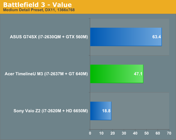
Nvidia “Kepler” GeForce GT 640M GPU Benchmarked in Acer M3 Ultrabook


Even though Nvidia hasn’t officially announced its 600-series of mobile GPUs based on the Kepler architecture, the first benchmarks of such a graphics core, the GeForce GT 640M, have already made their appearance on the web.

This 28nm GPU was used by Acer in its recently announced Aspire TimelineU M3 Ultrabook, which was reviewed by AnandTech just a few hours ago.

According to the specifications accompanying Acer’s notebook, the GT 640M graphics core runs at speeds up to 625MHz and includes no less than 384 CUDA cores.

This is four times the number of shaders packed by its predecessors, the GT 540, if we are to believe what Acer tells us.

In the TimelineU M3 Ultrabook , the GT 640 graphics core is linked via a 128-bit wide bus to 1GB of DDR3 memory that works at 900MHz (1.8GHz data rate), but Nvidia also allows for this GPU to be paired with faster GDDR5 VRAM.

Besides the Nvidia Kepler graphics card, Acer’s ultra-thin notebook also includes an Intel Core i7-2637M dual-core CPU with a base frequency of 1.7GHz and 2.8GHz maximum Turbo, as well as 4GB of dual-channel DDR3 memory.

The Ultrabook was put through various benchmarks, including Battlefield 3, Skyrim or Dirt 3, to test its gaming performance.

These have revealed that the GeForce GT 640M is a significant upgrade when compared with the GT 540M it replaces, as it manages to deliver playable frame rates in all of the games tested at the notebook’s default 1366x768 resolution.

So far, we don’t know when Nvidia plans to officially announce its new 600-series mobile GPUs based on the Kepler architecture.

The first desktop part based on this design, the GeForce GTX 680, is rumored to be launched on March 23.


Twitter Delicious Facebook Digg Stumbleupon Favorites More

 
Design by Free WordPress Themes | Bloggerized by Lasantha - Premium Blogger Themes | coupon codes
`